


Application of Diamond Wafers in Industry and Electronics
Diamond wafers, an advanced material composed of a thin layer of diamond deposited on a substrate, are transforming various sectors of industry and electronics.
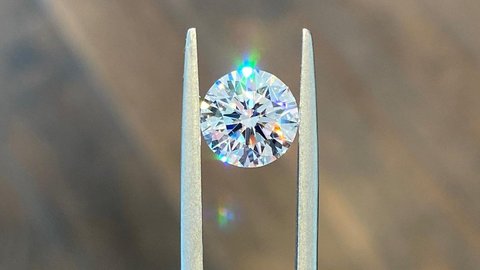
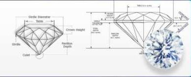
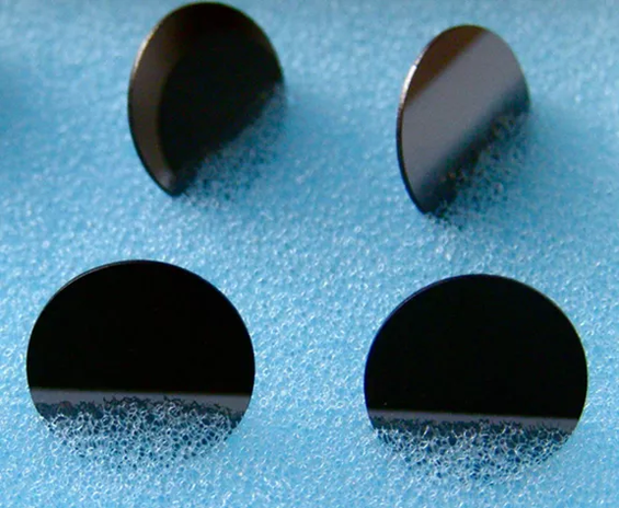
What is a Diamond Wafer?
A diamond wafer is a thin slice of diamond material that is used as a substrate for various applications in electronics and other industries.
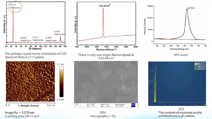
Diamond wafers can be produced using high-pressure, high-temperature cubic pressing (HPHT) or CVD methods.
Labrilliante provides a range of High Pressure High Temperature (HPHT) cubic press machines, with pricing tailored to specific customer requirements. The systems are designed with user-friendly interfaces and automated features, ensuring streamlined operation and minimal training time.
Get information on prices and availability
GaN-on-Diamond Semiconductor for Wireless Communication
One of the most promising applications of diamond wafers is in the field of wireless communication. GaN semiconductors, which consist of a thin layer of gallium nitride (GaN) deposited on a diamond substrate, have emerged as a superior alternative to traditional materials like silicon carbide (SiC).
GaN semiconductor offers several advantages, including:
- Increased power density. GaN-on-Diamond semiconductors can achieve power densities up to three times higher than GaN without diamond, enabling more compact and efficient devices.
- Improved reliability. The reduced thermal stress and strong atomic bonding between GaN and diamond enhance the overall reliability and longevity of the device.
- Superior high-frequency performance. The exceptional thermal conductivity of diamond allows GaN-on-Diamond devices to operate at higher frequencies without suffering from overheating issues.
These properties make GaN semiconductors an ideal choice for applications in high-power wireless communication devices, such as advanced 5G base stations, high-performance radar systems, and cutting-edge satellite communication equipment. The integration of GaN-on-Diamond technology in these fields enables the development of more efficient, reliable, and compact wireless communication solutions.
Diamond Wafers in AI & Cloud Computing
Diamond wafers are also making significant advancements in the realm of artificial intelligence (AI) and cloud computing. The integration of diamond wafers with high-power silicon chips creates a highly efficient thermal management solution that can accelerate computation by up to three times. The efficient heat dissipation provided by diamond wafers reduces hotspots and allows chips to operate at higher frequencies without overheating.
This technology is compatible with leading high-power chips, enabling data centers to achieve the same performance while occupying half the space, leading to substantial cost savings and energy efficiency improvements. The use of diamond wafers in AI and cloud computing can lead to faster processing speeds, improved energy efficiency, and reduced hardware costs.
The Diamond Wafer in Power Electronics
In the field of power electronics, diamond wafers are enabling significant advancements. The extreme thermal conductivity and electrical insulation properties of diamond allow for the simplification of inverter architectures, resulting in miniaturization, increased efficiency, and enhanced robustness.
Diamond wafers enable the development of compact, lightweight, and highly efficient power inverters, which find applications in various industries, including:
- Renewable energy. Diamond-based power electronics can improve the efficiency and reliability of solar and wind power systems.
- Electric vehicles. Compact and efficient diamond-based inverters can reduce the size and weight of electric vehicle powertrains.
- Aerospace. Diamond-based power electronics can withstand the harsh environments and high temperatures encountered in aerospace applications.
The advancements in diamond GaN technology have opened up new possibilities for the semiconductor industry. As the demand for high-performance, reliable, and compact wireless communication devices continues to grow, manufacturers are seeking cost-effective solutions to integrate diamond GaN into their products.
What are the Benefits of Using Diamond Wafers?
Diamond wafers have many advantages beyond their applications in wireless communication, AI and cloud computing, and power electronics. The material is characterized by these properties:
- Hardness and durability. Diamond is the hardest-known material, offering superior wear resistance and precision in cutting tools and machining applications.
- Optical properties. Diamond wafers provide excellent transparency and stability, which makes them suitable for lenses, and other optical components.
- Chemical inertness. This material is resistant to acids and other chemicals, allowing it to be used in harsh chemical environments.
- Biocompatibility. Diamond is biocompatible, making it an attractive material for medical devices and implants.
Diamond wafers are revolutionizing industry and electronics by offering a unique combination of properties that surpass those of traditional materials. They are revolutionizing industry and electronics by offering a unique combination of properties that surpass those of traditional materials.